Latest Advancements in MicroLED Fabrication
The path from research labs to market commercialization has been a long one for microLED displays. Challenges in mass fabrication have slowed the release of all but a few high-end products, such as Samsung’s “The Wall” television. However, some exciting recent developments are helping the industry move closer to mass market availability of microLED displays:
- LED pioneer Shuji Nakamura leads a team developing microLEDs with high External Quantum Efficiency. Working with semiconductor firm Seoul Viosys, Nobel-prize winner Nakamura and his team at the University of California Santa Barbara’s Solid State Lighting & Energy Electronics Center (SSLEEC) have developed blue and green LEDs of just 1µ diameter1 and red LEDs of <70 µm that overcome the quantum efficiency challenges. Using these techniques, Seoul Viosys plans to move rapidly into production of microLED displays for smart phones and AR/VR headsets. Learn more…
Nobel-prize winner Shuji Nakamura lectures on microLED technology and fabrication.
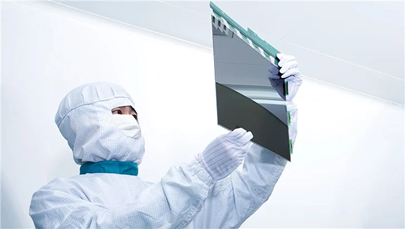
- Consumer electronics giant BOE has been working on a transfer printing technique to improve microLED yields. At this year’s CES show in January it unveiled a prototype active-matrix microLED screen fused into a glass substrate, enabling seamless tiling for larger panel sizes. Recently, the company announced it has been able to achieve mass production of microLED display panels from 8-inches to 12-inches at its plant in Kunming, China. Learn more…

MicroLED panel manufacturing. (Image: BOE)
- Pseudo substrates improve red microLED yield. – Standard red LEDs have phosphide-based structures. However, at the smallest LED sizes of <10µm, required for microLEDs used in applications such as AR/VR devices, performance and yields decrease significantly. French researchers have pioneered a new method2 of making red-emitting gallium nitride-based microLEDs that promises improved yields and energy efficiency. Learn more…
MicroLEDs Moving To Market
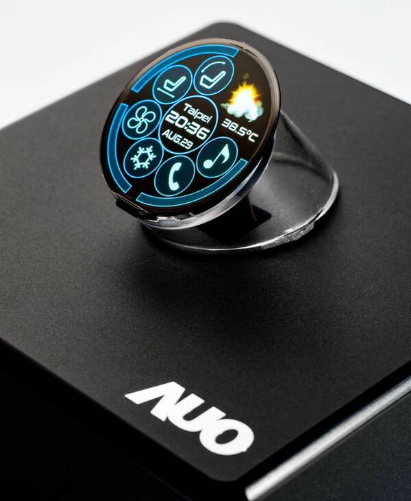
New microLED applications and prototypes are also helping build excitement and market momentum. For example, AUO recently unveiled a unique 1.39-inch, 338 ppi full-circle microLED display “featuring the highest resolution density in the world, which can be used with a center console for electric knob applications. Moreover, the gadget boasts a unique curvilinear cutting technique, allowing automobile manufacturing companies to customize solutions for diversified designs of different automotive dashboards, thereby enhancing driving intuitiveness and safety.”3

Full-circle display module from AUO, developed in partnership with PlayNitride, has potential applications for automotive, mobile devices/wearables, and more. (Image: AUO, Source)
Currently, several electronics manufacturers, including Samsung, LG, Sony, and Konka, have released microLED television models to the market, although they are still generally quite large (approximately 75” and up) and very expensive. Prices are typically in the six-figures range (>US$100K), well out of reach for the average consumer. Time will tell if microLED products will break through to commercialization, realized by one or more manufacturers who have teased exciting prototypes—AUO, PlayNitride, RiTdisplay, TCL, Tianma, Glo, Plessey, JBD, X-Display, VueReal, CSOT, Sharp, Kyocera, and others.4
Reflecting on these developments, leading industry analysts see these recent technical and scientific breakthroughs coupled with a surge of investment and patent filings pointing to market movement—with microLED displays soon to reach “escape velocity.”5
MicroLED Inspection Ensures Yields for Commercialization
One of the biggest production challenges for microLED display makers is mass transfer of individual microLED chips/chiplets onto a substrate to create screen panels. Hand-in-hand with these challenges is a need for efficient visual quality inspection with microscopic and near-microscopic precision.

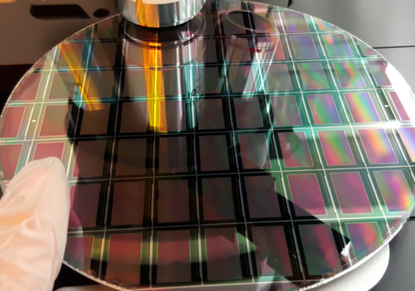
Plessy Semiconductors GaN on silicon microLED wafers in production. (Image: CC by SA 4.0)
Manufacturers typically need to verify quality at several stages in the development of a microLED display: from the LED chip and wafer stages through to module, panel, and final device assembly. At the individual LED level, in many cases luminance and color output must be so precisely measured that a microscope lens (a microscope objective) may be needed. This, paired with a photometric or colorimetric imaging device, ensures precise specifications for light and color output are met.
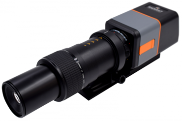
To ensure the absolute quality of microLED display devices, Radiant’s measurement solutions—ProMetric® Imaging Photometers and Colorimeters used alone or with our Microscope Lens—are enabling microLED manufacturers to asses display performance and uniformity down to the subpixel level, with accurate and repeatable results.

Radiant’s ProMetric® Y-series Imaging Photometer used with our Microscope Lens, which provides 5x and 10x magnification for extremely high-resolution subpixel inspection.
To learn more about the challenges of microLED fabrication and how companies are working to address them, read our article “Progress in MicroLED Fabrication and Quality: Closing the Commercialization Gap,” published by Manufacturing Tomorrow.

CITATIONS
- Smith, J., et al. “Comparison on size-dependent characteristics of blue and green InGaN microLEDs down to 1 m diameter,” Applied Physics Letter, vol. 116(7), February 19, 2020. DOI: https://doi.org/10.1063/1.5144819
- Dussaigne, A., et al. “Full InGaN (625 nm) micro-LED (10 µm) demonstration on a relaxed pseudo-substrate” Applied Physics Express vol. 14(9), September 3, 2021.
- “As Innovative MicroLED Applications Emerge, Overcoming Mass Transfer and Testing Problems is Top Priority.” LEDinside, July 29, 2021.
- “Micro-LED Displays from 2021 Onward Analyzed by IDTechEx.” CISION PR Newswire, July 15, 2021.
- “MicroLEDs show progress on all fronts: have they reached escape velocity?” Yole Développement Press Release, August 5, 2021.
Join Mailing List
Stay up to date on our latest products, blog content, and events.
Join our Mailing List
